



The chip select logic for a certain DRAM chip in a memory system design is shown below. Assume that the memory system has address lines denoted by to . What is the range of address (in hexadecimal) of the memory system that can get enabled by the chip select (CS) signal?
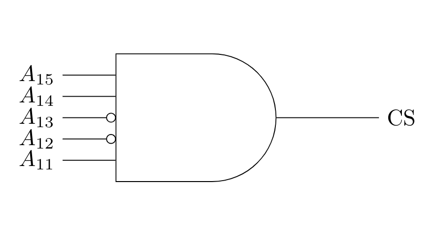
View worked solution
Answer: A
To find the enabled address range, we analyze the logic gates that generate the active-low chip select signal :
- An AND gate with inputs and produces the output .
- A NOR gate with inputs and produces the output .
- A 3-input NAND gate takes these two outputs along with to produce the active-low chip select signal:
For the DRAM chip to be enabled, we require . This is achieved when all inputs to the final NAND gate are :
- and
- and
Thus, the upper 5 address bits are fixed as . The remaining 11 bits ( to ) can vary freely from all s to all s:
- Minimum Address:
- Maximum Address:
Therefore, the address range is C800 to CFFF.
Free practice · Your answers on this page are not saved.