



In the three dimensional view of a silicon n-channel MOS transistor shown below, . The transistor is of width . The depletion width formed at every p-n junction is . The relative permittivities of and , respectively, are and , and .
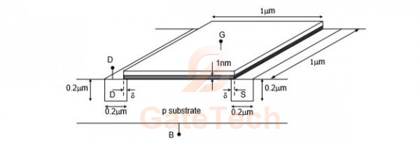
The gate-source overlap capacitance is approximately
View answer
Answer: A
Worked explanation not available yet.
Free practice · Your answers on this page are not saved.