Skip to content
Official PYQ · 2001

GATE EC 2001 Set 1 Q2.6 — BJT and MOSFET Amplifiers

Explain with AI

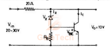
The transistor shunt regulator shown in the figure is has a regulated output voltage of 10 V10 \mathrm{~V}, when the input varies from 20 V20 \mathrm{~V} to 30 V30 \mathrm{~V}. The relevant parameters for the zener diode and the transistor are: VZ=9.5, VSE =0.3 V,β=99\mathrm{V}_{\text{Z}}=9.5, \mathrm{~V}_{\text{SE }}=0.3 \mathrm{~V}, \beta=99. Neglect the current through RBR_{B}. Then the maximum power dissipated in the zener diode (PZ)(\mathrm{P}_{\mathrm{Z}}) and the transistor (PT)(\mathrm{P}_{\mathrm{T}}) are

Choose one option
View answer

Answer: C

Worked explanation not available yet.

Free practice · Your answers on this page are not saved.

Published
Report a correction
Keep exploringMore BJT and MOSFET Amplifiers questions