



A silicon junction is shown in the figure. The doping in the region is and doping in the region is . The parameters given are
- Built-in voltage =
- Electron charge =
- Vacuum permittivity =
- Relative permittivity of silicon =
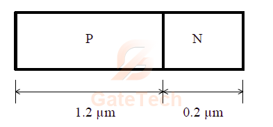
The magnitude of reverse bias voltage that would completely deplete one of the two regions ( or ) prior to the other (rounded off to one decimal place) is ______________________ .
View answer
Answer: 8.1:8.4
Worked explanation not available yet.
Free practice · Your answers on this page are not saved.