

Skip to content
Official PYQ · 2013

GATE EC 2013 Set 1 Q34 — Electronic Devices

Explain with AI

The small-signal resistance (i.e.,dVB/dID)(i.e., dV_{B}/dI_{D}) in kΩk\Omega offered by the nn-channel MOSFET MMOSFET\: M shown in the figure below, at a bias point of VB=2 VV_{B} = 2\: V is (device data for M:M: device transconductance parameter kN=μnCox′(W/L)=40 μA/V2,k_{N} = \mu_{n} C'_{ox} (W/L) = 40\: \mu A/V^{2},threshold voltage VTN=1 V,V_{TN} = 1\: V, and neglect body effect and channel length modulation effects) 
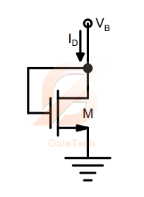
Choose one option
View answer

Answer: B

Worked explanation not available yet.

Free practice · Your answers on this page are not saved.

Published
Report a correction
Keep exploringMore Electronic Devices questions